Throwing light on to nanowires
At the École Polytechnique Fédérale de Lausanne (EPFL) in Switzerland, Professor Anna Fontcuberta i Morral’s ERC-funded UPCON project (Ultra-pure nanowire heterostructures and energy conversion) is investigating new concepts and technologies that point the way to the next generation of photovoltaic systems. Prof Fontcuberta i Morral is a speaker at this year's American Association for the Advancement of Science (AAAS) conference in Chicago, where she will give a talk entitled 'Nanowires have the power to revolutionize solar energy'.
Over the past 20 years, the growth of research into photovoltaic cells has been driven by the rising economic and environmental costs of fossil fuels. Even so, the unit-energy costs from photovoltaic sources remain relatively high. Therefore, innovative concepts and technologies are urgently needed to increase the overall efficiency of photovoltaic systems and reduce the costs of the energy they produce.
“Early photovoltaic cells used thick silicon semiconductor technologies which are limited to an energy-conversion efficiency of around 30-40 %,” explains Prof. Fontcuberta i Morral, “The second-generation devices use less material and rely on micron-scale thin-film silicon technologies. However, the theoretical energy-conversion limit – the efficiency of turning the sunlight falling on the surface into electrical energy – remains unchanged. Our aim is to use nanoscale technologies to overcome this limit and demonstrate devices that can provide a step change in the performance of photovoltaic devices.”
Of growing importance
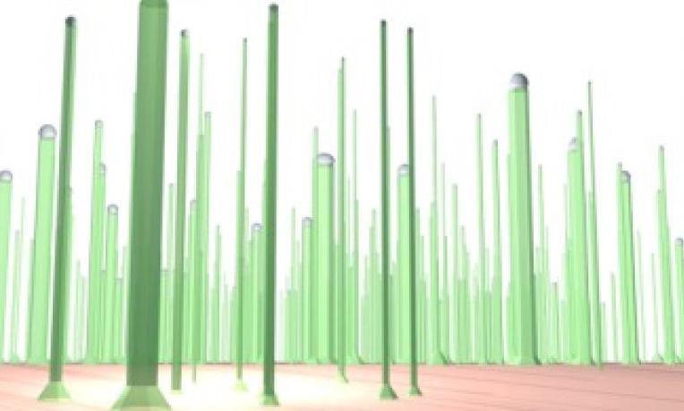
Prof. Fontcuberta i Morral and her team are investigating nanowire solar cells. Using molecular beam epitaxy, a technique used in making microchips and other electronic devices, they grow nanowires which are typically 50-300 nm in diameter and up to 30 microns long. These are grown vertically on a silicon substrate and are made of gallium arsenide layers which form ‘p-n junctions’ that convert incident light to electrical energy. The p-n junctions – interfaces between two types of semiconductor materials that form the basis of most electronic devices – can be either horizontal to the wire, or radial along its length.
Eventually, the intention is to grow two-dimensional arrays of nanowires, each separated from its neighbour, to produce ‘forests’ of individual solar cells. A vital aspect of this next-generation technology is scale, as the professor explains: “Moving solar-cell devices to the nanoscale brings eventual manufacturing cost savings, for example in the use of expensive materials. In addition, as the devices get smaller and the dimensions of the nanowires are smaller than the wavelength of the incident sunlight (400-700 nm), new physical phenomena come into play which can help break through the energy-conversion barriers that limit larger-scale devices.”
Lighting the way
In 2013, together with researchers from the Niels Bohr Institute in Denmark, Prof. Fontcuberta i Morral and her UPCON colleagues at the EPFL, Martin Heiss and Olivier Demichel, published their latest research results that demonstrate just how important the element of scale is.
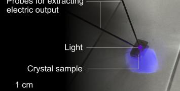
The research involved depositing a single, two-micron-long nanowire solar cell on to a silicon substrate and then measuring the light absorption and electrical current generated when it is illuminated. They found that, remarkably, light absorption in the vertical nanowire is much higher than in an equivalent thin-film solar cell, and the nanowire generates several times the electrical power. In fact, the nanowire absorbs light from an area that is larger than its physical cross-section – confirming that it has built-in light concentration properties. In effect, nanowire solar cells work as if they had small-scale lenses collecting light from a larger area. Solar cells become more efficient when working under such light-concentration conditions. Thus, this is a route to further increasing solar cell efficiency.
“This research shows that nanowire arrays offer a path for more efficient solar cells, and the increase in absorption cross-section means that they can be more widely spaced, thus greatly reducing material costs,” says Prof. Fontcuberta i Morral. As well as the experimental results, the team modelled the nanowires to understand how the efficiency boost arises as a function of wavelength and nanowire diameter. They found that, theoretically, absorption could be boosted by up to a factor of 70 times.
These recent and unexpected results are receiving much interest from the scientific community, partly due to the potential for future photovoltaic energy sources. However, as the professor points out, the implications are wider: “Our research concerns more than renewable energies. Small nanowire arrays could act as tiny power sources integrated into the nano-machines and devices of the future, such as health sensors for diseases like diabetes. They could be used as almost-free energy sources to produce hydrogen fuels from water, an expensive process at the moment. And equally, this is about doing more with less. It is increasingly important for material scientists to factor in the growing scarcity of strategic metals and minerals from the earth’s crust, so nanowire-based devices have the potential to raise overall efficiency, both in converting light to energy and in using less valuable resources to do so.”


